
Hover on the image to zoom
")
")
")
")
")
")
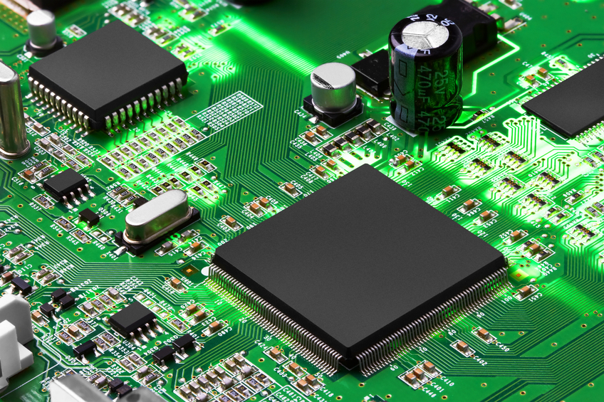
PCBA
- High Accuracy and Integration
- Systematization and Integration
- Customization
Contact
Specifications
Specifications
Describe
Definition and Function
A printed circuit board assembly (PCBA) is a PCB with all the necessary electronic components mounted and soldered onto it, forming a complete and functional circuit. The process of assembling a PCB with its components is known as PCB assembly, and it is a critical step in the production of electronic devices. The primary function of a PCBA is to provide a platform for the electronic components to work together in a coordinated manner, enabling the device to perform its intended tasks.
In more technical terms, a PCBA serves as the electrical interconnect that routes signals between components according to the schematic of the device. It also provides the necessary ground planes, voltage planes, and impedance control needed for stable electrical performance.
The assembly process involves placing and soldering components such as resistors, capacitors, integrated circuits, and connectors onto the PCB. This can be done using various techniques, including through-hole soldering and SMT, depending on the type of components and the design requirements of the device. Once the components are securely attached to the PCB, the assembled board is tested for functionality, quality, and reliability before being integrated into the final product.

The performance of a PCBA is influenced by several factors, including the quality of the components, the accuracy of the assembly process, and the integrity of the solder joints. These factors can impact the electrical characteristics of the assembled board, such as its resistance, capacitance, and inductance, as well as its overall reliability and lifespan. Therefore, it is essential to carefully select components, follow best practices for assembly, and thoroughly test the PCBA to ensure optimal performance and reliability in the final electronic device.
Types of PCBAs
PCBAs can be categorized based on various factors, such as the assembly technique used, the complexity of the circuit, and the intended application. The primary types of PCBAs include through-hole assembled PCBAs, surface-mount assembled PCBAs, and mixed-technology PCBAs.
Through-hole assembled PCBAs utilize through-hole components, which have leads that are inserted into holes drilled into the PCB and soldered on the opposite side. This assembly technique has been widely used for decades and is known for its robust mechanical connections and ease of prototyping. However, through-hole components are generally larger and require more space on the PCB, making them less suitable for high-density and miniaturized designs. Through-hole assembled PCBAs are commonly found in older electronic devices, power electronics, and applications where strong mechanical connections are required.
Surface-mount assembled PCBAs employ SMT, where components with solder pads are placed directly onto the PCB and soldered to the traces using a reflow soldering process. SMT components are smaller and can be mounted on both sides of the PCB, allowing for higher component density and more compact designs. Surface-mount assembled PCBAs are widely used in modern electronics, such as smartphones, computers, and IoT devices, due to their improved performance characteristics and space-saving advantages.
Mixed-technology PCBAs combine both through-hole and surface-mount components on the same board, taking advantage of the strengths of each assembly technique. This approach is often used when specific components are only available in one form factor or when the design requirements call for a combination of the mechanical robustness of through-hole connections and the high-density capabilities of surface-mount technology. Mixed-technology PCBAs can be found in a variety of applications, including industrial controls, automotive electronics, and medical devices.

In addition to these, there are several other types of assemblies such as flexible PCBAs, and Ball Grid Array (BGA) PCBAs. Flex PCBAs are designed to bend and flex, making them ideal for applications where space constraints are a concern or where the PCB needs to conform to a particular shape. BGA PCBAs, on the other hand, utilize a surface mount packaging technique for integrated circuits, offering a compact footprint, high lead count, and enhanced thermal and electrical performance. These specialized PCB types are often utilized in devices requiring intricate designs and high flexibility, such as in aerospace, medical devices, and high-performance computing applications.
The choice of which type of PCBA to use depends on factors such as the design requirements, the available components, the desired performance characteristics, and the project’s budget. By understanding the differences between these types of PCBAs, engineers and designers can make informed decisions that best meet the needs of their specific applications.
PCBA Manufacturing Process
The PCBA manufacturing process involves several stages, including PCB fabrication, component procurement, and assembly. Each stage plays a critical role in ensuring the functionality, reliability, and performance of the final assembled board. It’s also important to note that the foundation of a PCBA is the PCB; without a PCB, a PCBA cannot be created.
PCB Fabrication:
As discussed in the PCB manufacturing process, the fabrication stage involves creating the physical PCB based on the design files. This includes etching the copper traces, drilling holes for through-hole components and vias, and applying solder mask and silkscreen layers. The fabricated PCB serves as the foundation for the assembly process.
Component Procurement:
efore assembly, all the necessary electronic components must be procured. This involves selecting and sourcing components based on the design requirements, such as performance specifications, form factor, and cost. Component procurement is a critical step, as the quality and availability of components can directly impact the performance and lead time of the PCBA.
For high-frequency applications, material selection becomes critical. Materials like Rogers or polytetrafluoroethylene (PTFE) laminates are often used to minimize signal loss. Additionally, the manufacturing process may include impedance control measures and multi-stage inspections to ensure signal integrity.
Assembly:
he assembly process involves mounting and soldering the electronic components onto the PCB. This can be done using through-hole soldering, surface-mount technology (SMT), or a combination of both techniques, depending on the design requirements and the types of components used. The assembly process typically involves the following steps.
Stencil Printing:
A stencil is used to apply solder paste onto the PCB in precise locations where the surface-mount components will be placed. The solder paste contains tiny solder particles suspended in a flux medium, which helps to create strong and reliable solder joints during the reflow soldering process.
Component Placement:
Using automated pick-and-place machines, surface-mount components are accurately placed onto the PCB, aligning their solder pads with the corresponding solder paste deposits. For through-hole components, manual or automated insertion machines are used to insert the leads into the drilled holes.
Reflow Soldering:
The PCB, with surface-mount components in place, is passed through a reflow oven, where it is subjected to a controlled temperature profile. The solder paste melts and forms a solid connection between the component pads and the PCB traces. For through-hole components, wave soldering or selective soldering techniques are used to create solder joints.
Inspection and Testing:
After the assembly process, the PCBA is inspected for defects, such as misaligned components, solder bridges, or missing solder joints. Inspection methods include visual inspection, automated optical inspection (AOI), and X-ray inspection. The PCBA is also tested for functionality and performance using techniques such as in-circuit testing (ICT) and functional testing.
By understanding the intricacies of the PCBA manufacturing process, engineers and designers can make informed decisions that optimize the performance, cost, and manufacturability of their assembled boards. This knowledge can also help identify potential issues and implement best practices to ensure the highest quality and reliability of the final electronic device.
qcv –
sdsds
ffdf